The current development of Photonic Integrated Circuits, abbreviated to PICs, represent a photonics revolution that can bring more speed, lower costs and space savings. They are particularly attractive for high-volume applications, for example in the areas of data centers, autonomous driving or biosensors. However, in addition to many advantages, the technology also brings new challenges in terms of assembly, packaging and testing. Helbling's interdisciplinary development teams are geared towards integrating precisely such issues into the design process from the outset.
What are PICs and why are they useful?
When electronic circuits went from large boards to small, fully integrated chips, it was a technology revolution that made everything smaller, cheaper and faster. The same revolution is happening right now in photonics. To date, photonics-based devices have tended to be rather bulky and expensive because they consist of multiple optical elements that often need to be assembled manually. However, this new technology, known as photonic integrated circuits (PICs for short), facilitates the integration of photonics on a chip. This opens up new possibilities, not only in terms of cheaper, smaller and faster devices, but also for new functionalities that did not exist before, such as arrayed waveguide gratings for optical multiplexing, e.g., in the field of communications engineering or ring resonators for very narrow bandpass filters, e.g., in laser technology.
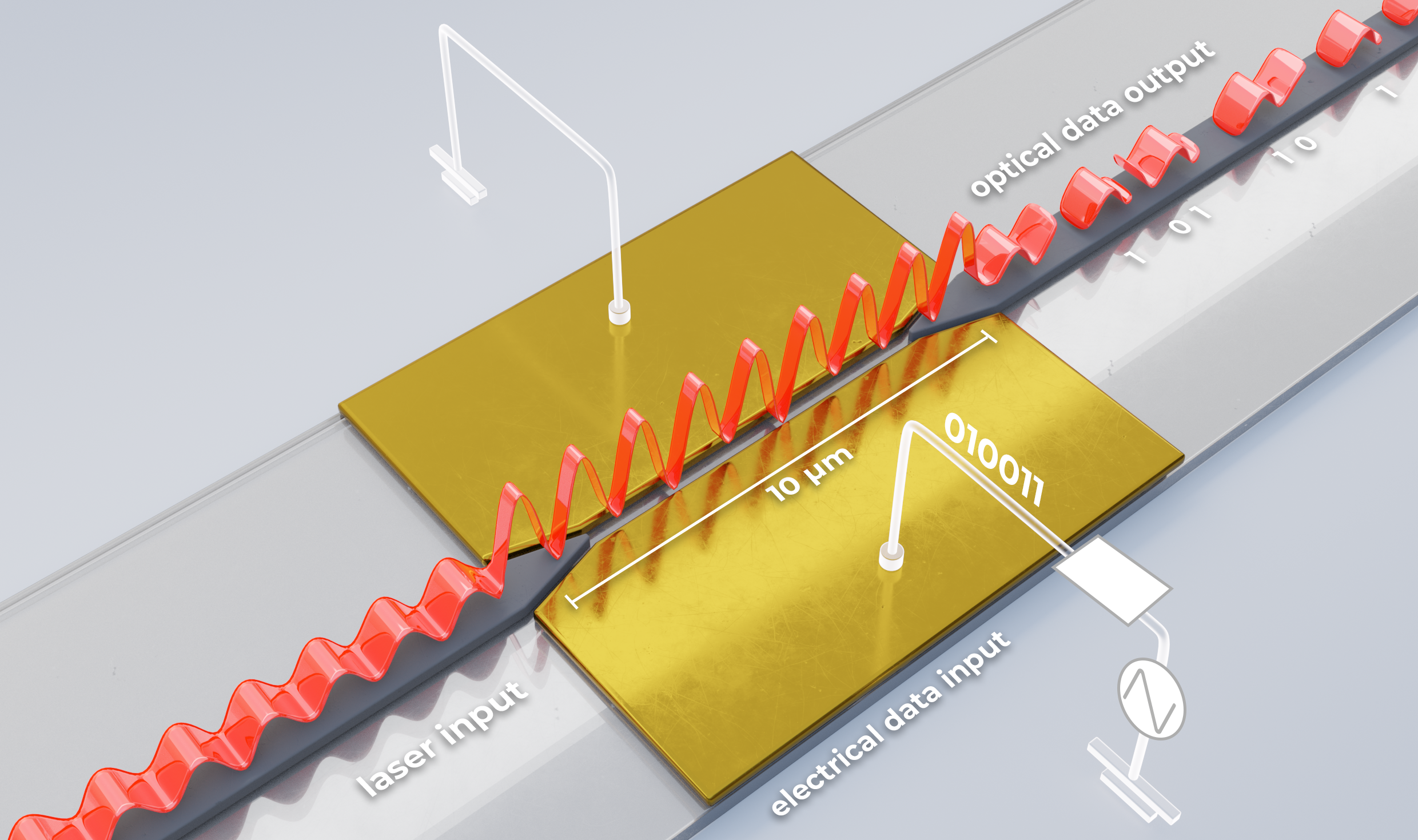
Like electronic chips, PICs have multiple optical functionalities integrated on a single chip with waveguides connecting the different elements. But unlike electronic chips, where silicon is the dominant material, PICs can consist of a wide range of different materials. In addition to silicon, typical materials can also include silicon on insulator, indium phosphate, silicon nitride and lithium niobate.
Application examples are still rare
Today, PICs are already commercially used in telecom and data center applications. PIC-based optical transceivers are much faster than traditional devices while consuming significantly less energy, therefore addressing two of the main challenges that data centers are facing in today’s world. For example, Intel provides optical transceivers with 400 Gb/s and has already announced an 800 Gb/s version.
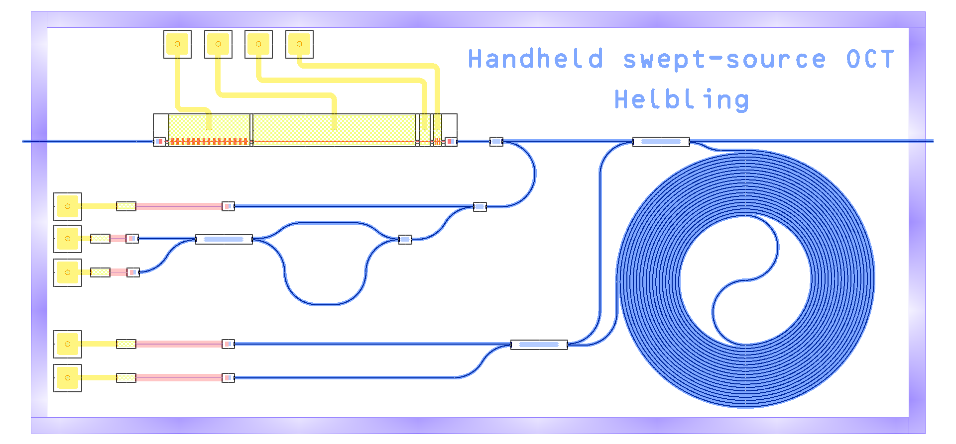
PICs are also gaining traction in other fields. However, these options have not yet been commercially exploited. There is still great potential here, for example as platforms for low-cost rugged LIDARs for autonomous driving, biosensors in healthcare devices such as point-of-care and home-use devices, and quantum computing systems. For example, the small form factor and low cost of PICs make them suitable for a miniaturized optical coherence tomography system used in handheld devices – an area where Helbling has already gained experience with corresponding concepts.
Developing devices with PICs requires a holistic approach
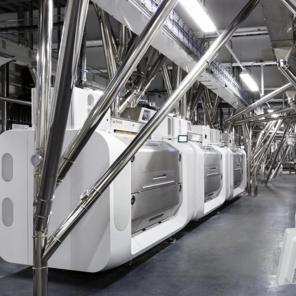
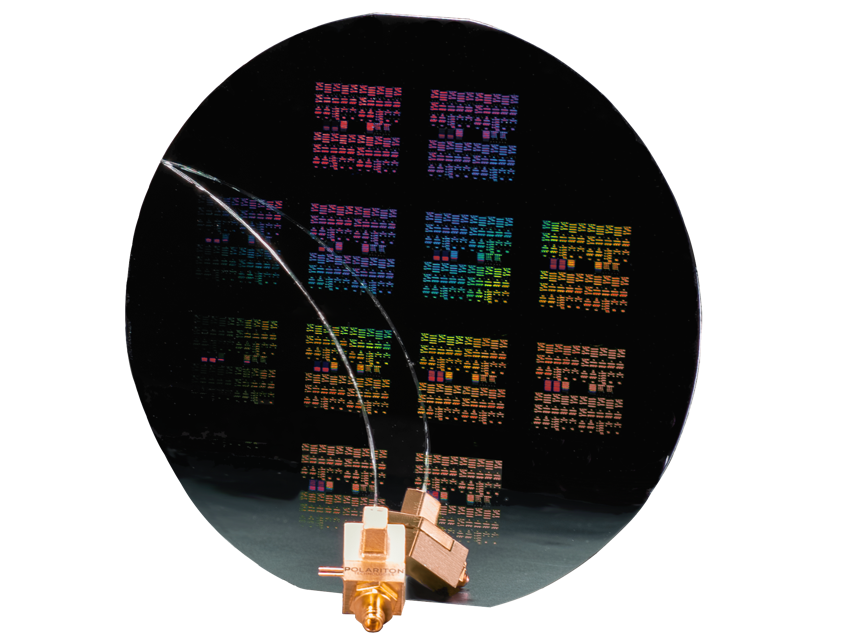
PICs are produced in wafer-based processes, which makes them particularly attractive for high-volume applications. The production method for the chips makes use of pre-existing electronic chip manufacturing technologies, which already works reliably for photonic chips too. Contemporary challenges in relation to manufacturing PICs are mainly centered upon assembly, packaging and testing processes. A chip is just a chip and cannot be used unless it is packaged and integrated into a device. High production volumes require automated manufacturing processes, especially with a view to keeping production costs low. For assembly and packaging, the PIC industry benefits from existing electronics production facilities to a limited extent, as many processes and tools need to be specifically developed to meet the demands of a PIC device.
These production aspects need to be considered from the beginning of the PIC development, starting with fundamental decisions on the system architecture of the device. Which functions does the device have and which of them can and should be integrated into the chip and which ones are better off being kept as external elements? What kind of interfaces are needed? It is crucial to not only consider optical inputs and outputs, but also electrical, mechanical and thermal interfaces. Answering these questions is essential to developing a high-performance device that also can be assembled and packaged in a sensible way. Assembly and packaging, but also testing for quality control, impose requirements on the PIC design; ignoring them will result in a chip that is not manufacturable or very expensive in terms of production. The starting point should therefore be a solid system architecture for the chip that takes into account all manufacturing aspects too. Helbling’s broad interdisciplinary competences, which cover optics, electronics, microtechnology, production technology and many more, provide a solid basis for developing the system architecture for PIC-based devices.
Multiple challenges in terms of integrating and packaging PICs
The requirements for PIC packaging differ from those of classical ICs, prompting the need for new machines, production equipment, activation procedures, and quality control steps.
1. Challenges in integration/packaging
PIC packaging mandates distinct optical and electrical interfaces for seamless connectivity to fibers or free-space optics, as well as power supplies and high-speed signal transmission. This necessitates meticulous planning during the PIC design phase, ensuring a layout conducive to accessibility for assembly and production interfaces, accommodating needles and fibers.
2. Challenges in assembly
The complex process often involves the active alignment of optical components, followed by UV glue hardening while the PIC remains connected to power, data, and optical input/output. The sheer diversity in PIC designs poses a challenge in devising highly adaptable machine concepts, requiring numerous fast-moving axes to achieve optimal throughput.
3. Challenges in testing
Efficient testing demands the re-establishment of both optical and electrical contacts to conduct performance assessments or burn-in procedures. To mitigate equipment costs, consideration must be given to consolidating assembly and testing within the same process step, leveraging highly flexible machinery for streamlined operations.
From a production machine standpoint, the development of novel features is essential. Designing fast, flexible machines that meet particle-free environment standards is crucial. Helbling is capable of supporting customers within the semiconductor and photonics market by offering expertise in the development of production equipment tailored to these demanding requirements.
Summary: Clever PIC design processes provide considerable added value
PICs mark a revolution in photonics. But to fully realize the benefits of this technology, certain production aspects pose challenges that must be taken into consideration. It all starts with fundamental decisions on the system architecture of the device. With its expertise in the fields of optics and mechatronics, Helbling is well-placed to develop the device with the PIC itself, as well as the process equipment for PIC assembly and packaging.
Authors: Helen Wächter Fischer, Fabian Schneider
Main Image: iStock